Thursday, 17 October 2013

Verilog code square root of a number using IP core

Hello friends after a long gap i am writing a new post as i was keeping busy with some other work.
I received about 12 mails asking for Verilog code to find square root of a number so thought of writing is small post to find sqrt of a number

   Here we will use the IP core from the Xilinx tool box and hoping that this module is just a part of your design and not the main project.
Create a new Verilog module and name is as " sqrt" or any another name which will help you identify the module easily.

Follow these steps

  1. create a new Verilog project 
  2. Right click on the module created and click on new New Source 
  3. select the IP (core generator and architecture wizard) > give  a name to the core ex. sqrt
  4. Go to Math Function >Square Root>Cordic 4.0 select the core and click next
  5. select the Square Root option and set the pipe lining mode to maximum and click next.
  6. select data format > unsigned integer(u can use floating if you require floating point sqrt).
  7. set round mode to truncate, this will give you the nearest square root of the number and click next.
  8. click on generate.
these are the snapshots which may help you to follow though the IP core generation process


After completing the IP core generation process declare the i/p and o/p ports in your main module or u can just copy paste this piece of code :

// copy from here
module sqrt(
x_in,
x_out,
clk
    );
 
input [15:0]x_in;
output [8:0]x_out;
input clk;
// PASTE YOUR INSTANCE OF IP CORE HERE
endmodule 
// end of copy

Now the next step is to paste the IP core instance to connect your main module ports to the IP core. you can get the IP instance as a file with extension as .VEO file. This instance can also be generated without the need to find the file with .veo extension. Just go the implementation mode from simulation mode and click on the IP core . In the process window you will find the instance code as shown below . Copy the instance and paste is immediately after the main code


After completing this process your final code must look like this :

//
module sqrt(
x_in,
x_out,
clk
    );

input [15:0]x_in;
output [8:0]x_out;
input clk;

//instance copied now
sqare_root YourInstanceName (
.x_in(x_in), // input [15 : 0] x_in
.x_out(x_out), // ouput [8 : 0] x_out
.clk(clk)); // input clk

endmodule
//

Well you are done. We are left with only the function verification which we can do with simulation, 
Try testing your module with different value and check if its working fine . 

Here is the simulation results which i have got for few values and the IP works perfectly fine


You can try with i/p which do not produce the perfect whole number and you may notice that the IP truncates the square root to nearest number . 

I hope you will like the post , though it was quite brief  :p . do let me know if there is anything you did not understand . 
 have a great day :-)
Also have a look at this new course : 


Link for the coupons : HeRE 

Tuesday, 1 October 2013

Linear Feed Back Shift Registers Using Verilog

Hie ,Here is yet another post about VLSI testing. In the last post we discussed about the testing of sequential circuits with the help of Scan Cells. Lets assume if we had the input bits to be some 100 bits long . In such a situation its again a nightmare to manually enter the inputs to the circuit under test and which is not practical too. Various test patterns generators have been proposed to trigger the inputs to the Circuit Under Test(CUT) which will produce random patterns for every clock cycle and reduces the burden to manually insert these as inputs to the CUT.    Figure below Shows the general scheme to test any circuit


     The Control Unit is responsible to coordinate the operation of the testing circuit.When the MUX select signal is HIGH (1) The circuit is said to be in the TEST mode or else its in the normal mode.Under Test mode the input to the CUT is from the Test Pattern Generator which will apply the test vectors to the CUT to be tested. The output response of the CUT are compared with the fault free response to declare the CUT as fault or fault free. In this post we will discuss about the Test Generators(TG) and the remaining blocks will be explained in my next post. 
      The choice of TG is an important criteria to ensure high fault coverage for the CUT and to make sure the circuit is working or not. Pattern generators like LFSR(Linear Feed Back Shift Registers ) can produce random patterns with low hardware requirements and is preferred choice for testing. It is categorized under pseudo-random test pattern generators which can produce a random pattern for every clock cycle applied to it. The figure below shows the general structure for a LFSR


     It consist of D-FF connected in cascade as shown with the same clock applied to all the FF to make them act like a shift register. But the only change is that the input to the first (D3 in th figure) is from the XOR of the o/p from FF's 0 and 3 (from fig). This XOR operation introduces a new  bit into the shift register .When we take out the output of these FF they will have a random pattern. This is a general structure for a 4 bit LFSR. The inputs to the XOR are called the Taps. So from the figure above the Taps are 0 and 3 FF's. There is no such order from where the inputs to the XOR comes from to produce a random pattern. But the pattern has to be of maximum length . By maximum length we mean that the pattern must repeat itself after 2^N clock cycles for a N bit LFSR. In our example if the LFSR has to be of maximum length then the pattern has to repeat after 16(2^4) clock cycles. For a small LFSR like the present one (4bit) its easy to identify the Taps to the XOR gate which can produce maximum length output but just imagine how can we identify the Taps for the XOR if the number of bits is 10bits ? Obviously we cant go by BRUTE FORCE method by trying all possible combination to identify the Taps which will produce maximum length sequence. Figure below shows the maximum length sequence produced by a 4 bit LFSR.


     You can notice that after 16 cycles the pattern is repeating for the LFSR. The Tap identification is the major criteria to produce a sequence like this which will repeat after 2^N clock cycles.But the fact is that the inputs for a CUT cannot be practically more than 128 bits or so. Xilinx has documented the Taps to be given for a given LFSR up to 165 bits. This makes the task for coding for LFSR by just using DFF and XOR gates with the Taps given by the Xilinx documentation. With these basics we can now proceed to design a LFSR for TG used in testing.

Design :
Components Required for Design : 
  • D-Flip Flops
  • XOR Gates
To illustrate the concept of LFSR and maximun length sequecne we will 4 bit LFSR. The Taps according to the Xilinx Document to produce a 6 bit maximum length sequence are 4 & 3(i.e the inputs to the XOR gate are from output of FF number 4 and 3). Figure below shows the RTL of the 4 bit LFSR.

                                                                        RTL


    You can notice that the inputs to the XOR gate are from o/p for DFF 4 and 3 and the output of this XOR gate is fed as input to the first FF. Figure below shows the simulation results of 4 bit LFSR which produces random patterns and which repeats exactly after 16 clock cyles.

                                                                 SIMULATION 


CODE

module lfsr_N_1(

d,
q,
rst,
clk
    );
parameter N=3;//given N one less than the number of FF in your design
input clk;
input d;
input rst;
output [0:N]q;
reg [0:N]q;

always@(posedge clk)

begin
 if(rst && d)
q<=1'b1;
else
4'b011:q={q[N]^q[N-1],q[0:N-1]};    //change the taps here for your design
end
endmodule


Advantages:
  • Low hardware 
  • Maximum length sequence can be produced 
  • Used for BIST
If you want to code for a N bit LFSR where N can be any number from 3 to 165 all you need to do is to declare a parameter N and write you code for the LFSR with Taps from the Xilinx Document. The links to the Xilinx Document and the references are given below


References:
This is our new course, happy learning


Link for the coupons : Here


Note: The code above works for only 4 bit, To make it work for any given N bit just change the Tap inputs. And the memory format used for coding is big endian format and you make change it to little endian format

Friday, 27 September 2013

Testing Of Sequential Circuits Using Verilog


Testing is the major challenge for any VLSI design either analog or digital. And it’s something which cannot be ignored or compromised with. Before your design gets converted to a product you must be very sure about the types of problems which may occur before hand. Just think of a scenario where I have my design which performs ALU operations and we will assume that we have made this design a product without testing it. Though the simulation version of the design may work well it’s not completely enough to declare the design as fault free. There can be N number of hardware faults which may occur within the circuit and following which your design may not work as per your expectation. For digital circuits hardware testing of your design can be done with FPGA based platforms (Spartan, vertex, etc). But the question is, are you sure that the FPGA implemented design will assure fault free designs after you plan to make your product? The answers is no. FPGA may give you the hardware platform to check your design functionality but when you want to convert this design of yours into a real circuit it may have some physical faults(strictly speaking about integrated circuits).
We will now try and establish an indirect means by which we can test any sequential circuit by making some modification to our design.This example below will help you understand the work better.
                                                          FIGURE 1


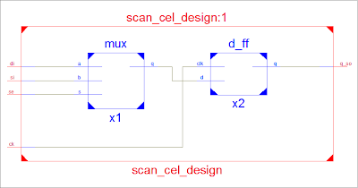
The circuit above is a simple sequential circuit and the gate (circled) has to be tested now. And as you can notice that we cant directly apply inputs to this gate because its not directly connected to the primary inputs. And you can notice that the FF are converted to Scan cells which were previously D-FF. The figure below shows how a D-FF can be converted to a Scan cell which will help us to test any Gate within the circuit which are not directly accessible.  


So to test any sequential circuits we have to replace all the D-FF to scan cell as shown in the figure.
Scan Cell Design:  It can operate in 2 modes 
  1. Normal mode where the SE(scan enable signal) is LOW and circuit and input is read from primary inputs
  2. Test mode where SE is high and can use this mode to test the internal gates and input is read from SI(scan inputs)
When SE is HIGH all the Scan Cells in the design are connected in series and when this connection of flops in series make them act like shift registers. And when SE in HIGH you can apply the test inputs one by one . In our design (FIGURE 1) the gate (Circled) has to be tested now. For this we have to apply both inputs to the AND gate as high and check if the output is HIGH . If its high than we can say that the Gate is fault free or else its faulty.Follow  the steps below to apply the test inputs to this gate and capture the response of this gate and verify your design.

Step 1: Make SE high (Now the scan cells act like shift registers)
Step 2:Apply test inputs to SI=1 and apply one clock. (this sets the output of first scan cell (X1 in figure 1) to 1.
Step 3: Apply SI=0. and apply one clock cycle .(this shifts output of X1 to X2 and sets output of X1 to 0).
Step 4: Apply SI=1. and apply one clock cycle.(this shifts output of X1 to X2 and output of X2 to X3 and output of X1 to 0)
Now if you observe that after step 4 we have actually set the outputs of scan cell X1 X2 and X3 to 1 , 0 and 1 respectively. 
                               

And indirectly we have applied 1 and 1 at the input to out AND gate :-) which we could not do before for any internal gates. The step after applying test input(11) to the Gate under consideration we have to check the Gates response now. Follow the steps below to capture the response of the gate.

Step 5: Make SE=0(normal mode) with primary inputs.
Step 6: Apply once clock cycle (this will make the scan cell X2 capture the response of our AND gate )
Step 7: Make SE=1(scan mode) apply one clock cycle (the caputured response of gate in X2 will we available at scan out. If the Gate is faulty the response will be 0 else it will be one.

The Simulation results for testing the AND gate is given below.


Advantages of Scan Cell 
  •  We can test sequential circuits 
  • Increases the control ability and make the circuit internal nodes more observable 
The Circuits are simulated using ISE and designed using Verilog

Have a look at this new course. 


Link for the coupons : Here


Saturday, 21 September 2013

Barrel Shifter design using 2:1 Mux Using Verilog


RTL SCHEMATIC


SIMULATION RESULTS 


CODE


 To Download:Click On the PDF and press (CNTRL+S)


BLOCK USED FOR IMPLEMENTATION 


EXPLANATION :
          Barrel sifter which are triggered using clock operate sequentially. For a shift or rotate of  N bits you will have to apply N clock cycles. Mux can be used to make the shift/rotate operation faster by converting the sequential circuit to computational logic. Just by application of a single clock cycle N shift/rotate can be done. The circuit used for implementation above is a simple configuration for rotate right operation. If you want to customize the design for shift(right/left) or rotate(R/L) the select line connection has to be changed accordingly. Also have a look at our exciting new course for free


Link for the coupons : Her

Friday, 20 September 2013

Carry select Adder using Verilog


                                                           RTL SCHEMATIC


SIMULATION RESULTS


                                                                   CODE


 To Download:Click On the PDF and press (CNTRL+S)


BLOCK DIAGRAM FOR IMPLEMENTATION 


Advantages : 
  • No need to wait for carry in every stage
  • Once the carry is known immediately the result can be obtained
  • Low delay of just 3 Ripple Carry Adders
I have been getting lot of mail & requests to provide the test bench also for CSA. Here is the Test feature module for CSA for you :


module test_csa;

// Inputs
reg [3:0] a;
reg [3:0] b;
reg cin;

// Outputs
wire [3:0] sum;
wire co;

// Instantiate the Unit Under Test (UUT)
carry_select uut (
.a(a), 
.b(b), 
.cin(cin), 
.sum(sum), 
.co(co)
);

initial begin
// Initialize Inputs
a = 0;
b = 0;
cin = 0;
#100;

a = 4'd5;
b = 4'd10;
cin = 0;
#100;

a = 4'd5;
b = 4'd10;
cin = 1;
#100;


a = 4'd15;
b = 4'd10;
cin = 0;
#100;


a = 4'd15;
b = 4'd11;
cin = 1;
#100;


// Add stimulus here

end

endmodule


Also look at our exciting new course


Link for the coupons : Here

Wednesday, 18 September 2013

Discrete cosine transform using verilog (DCT)


module dct1(sel,y);
  input [2:0]sel;
  output reg [15:0]y; 
  wire [15:0]y0,y1,y2,y3,y4,y5,y6,y7;
  wire [7:0]p0,p1,p2,p3,p10,p11,p100,m0,m1,m2,m3,m10,m11,m100;
  wire [15:0]n0,n1,n2,n3,q0,q1,q2,q3;
  wire [7:0]x0,x1,x2,x3,x4,x5,x6,x7;

// pre declared
parameter c1=8'b11111011;
parameter c2=8'b11101100;
parameter c3=8'b11010100;
parameter c4=8'b10110101;
parameter c5=8'b10001110;
parameter c6=8'b01100001;
parameter c7=8'b00110001;

// pre declared
assign x0=8'b10110;
assign x1=8'b1001;
assign x2=8'b101;
assign x3=8'b1111;
assign x4=8'b1011;
assign x5=8'b10;
assign x6=8'b100;
assign x7=8'b10010;

//Butter Fly Stages


//stage1
bfly1 s11(x0,x7,p0,m0);
bfly1 s12(x3,x4,p1,m1);
bfly1 s13(x1,x6,p2,m2); 
bfly1 s14(x2,x5,p3,m3);
//stage2
bfly2 s21(m0,m1,c1,c7,n0,q0); 
bfly2 s22(m2,m3,c3,c5,n1,q1);
bfly2 s23(m0,m1,c5,c3,n2,q2);
bfly2 s24(m2,m3,c7,c1,n3,q3);
bfly1 s15(p0,p1,p10,m10);
bfly1 s16(p2,p3,p11,m11);
//stage3
bfly2 s31(m10,m11,c2,c6,y2,y6);
bfly1 s32(p10,p11,p100,m100);

assign y1=n0+n1;
assign y7=q0+(~q1+1);
assign y5=n2+(~q3+1);
assign y3=q2+(~n3+1);
assign y0=p100*c4;
assign y4=m100*c4;


always@(sel)
case(sel)
  0:begin y=y0; end
  1:begin y=y1; end
  2:begin y=y2; end
  3:begin y=y3; end
  4:begin y=y4; end
  5:begin y=y5; end
  6:begin y=y6; end
  7:begin y=y7; end
endcase
 endmodule

module bfly1(x,y,p,m);
  input [7:0]x,y;
  output[7:0]p,m;
  assign p=x+y;
  assign m=x+(~y+1);
  endmodule

module bfly2(x,y,cx,cy,sx,sy);
  input [7:0]x,y,cx,cy;
  output [15:0]sx,sy;
   assign sx=(x*cx)+(y*cy);
  assign sy=(x*cy)+(~(y*cx)+1);

endmodule


Link for the coupons : Here

THE ABOVE DESIGN IS FOR 8 POINT DCT

Tuesday, 10 September 2013

Types pf flip flops with Verilog code

Flip flop are basic storage elements and the soul for sequential circuit design. Based on the application & the need we can design and use a flip flop. Few of the flip flops which are usually used for sequential circuits and for memory design are

You can code for any given FF with the truth table and thereby converting them into a logic gate configuration which is quite a simple task as far as these flip flops are concerned.


*********************************************************************************
SR-FF

     Characteristic equation: Q(next) = S + R'Q ,SR = 0

S
R
Q(next)
0
0
Q
0
1
0
1
0
1
1
1
undefined

From the truth table its clear that the FF has two inputs. S & R represents Set & Reset respectively. To model this FF we can use the CASE statement and define all the four input combination and the related output .Its always a good design to have a reset for your FF so as to bring it to a defined stage at any point of time asynchronously. If your design requires the use of output and its compliment then it can also be defined in your code as follows:

Verilog code for SR Flip-Flop

module srff(s,r,clk,rst, q,qb);
    input s,r,clk,rst;
    output q,qb;
               reg q,qb; 
              reg [1:0]sr;
             always@(posedge clk,posedge rst)
            begin
             sr={s,r}; //concatenate S&R to a 2 bit value
             if(rst==0) // when reset is not asserted
                        begin
                        case (sr)
                        2'd1:q=1'b0;
                        2'd2:q=1'b1;
                        2'd3:q=1'b1;
                        default: begin end
                        endcase
                        end
            else                              // when reset is asserted 
            begin
                        q=1'b0;
                        end
                       
                        qb=~q;
                        end
 endmodule

 In the above design you must have noticed that the input combination "11" is also defined which is not true in case of SR FF as its a undetermined state. To correct the design u can model the same using gate level coding using NAND or NOR gates as shown using the inbuilt function   nand(); available in the library.


*********************************************************************************


*********************************************************************************
J-K FF
     Q(next) = JQ' + K'Q

J
K
Q(next)
0
0
Q
0
1
0
1
0
1
1
1
Q'(toggle)

 This one is similar to the SR FF except that the "11" state defines a state where the output toggles between 1 & 0.  The same design for SR can be extended with two more nand gates to define the JK.


Verilog code for JK Flip Flop

`define TICK #2 //Flip-flop time delay 2 units
module jkflop(j,k,clk,rst,q);
input j,k,clk,rst;
output q;
reg q;
always @(posedge clk)begin
if(j==1 & k==1 & rst==0)begin
q =`TICK ~q; //Toggles
end
else if(j==1 & k==0 & rst==0)begin
q = `TICK 1; //Set
end
else if(j==0 & k==1)begin
q = `TICK 0; //Cleared
end
end
always @(posedge rst)begin
q = 0; //The reset normally has negligible delay and hence ignored.
end
 endmodule


The above code defines the time delay also for the FF.

********************************************************************************* 


Link for the coupons : Here


********************************************************************************* 

D-FF
                            Q(next) = D 
D
Q(next)
0
0
1
1

This one is the simplest of all the FF and also easy to model . Though its the simplest one its the most used FF for designs.

Verilog Code for D-Flip Flop

// code for dff
module Dff(input d,input clk,output reg q);
  always @(posedge clk) // note: lines whithin the always block are executed sequententialy 
  begin
  q=d;
  end 
endmodule

// code ends

 *********************************************************************************


*********************************************************************************
T-FF
                              Q(next) = TQ' + T'Q
T
Q(next)
0
Q
1
Q'
 This one is the next simplest FF after D. Here the output is  retains the previous state when input is 0. And when the input is 1 the output toggles i.e for every rising edge of the clock when input is 1 the output toggles from its previous value.

Verilog code for T flip flop

module tff_sync_reset (
data  , // Data Input
clk   , // Clock Input
reset , // Reset input
q       // Q output
);
input data, clk, reset ;
output q;
reg q;
always @ ( posedge clk)
if (~reset) begin
  q <= 1'b0;
end else if (data) begin
  q <= !q;
end
*********************************************************************************