FSM DESIGN MADE SIMPLE
Hie, its been a long time since i updated my blog as i was busy with other projects. In last one month i have received many requests to provide the more details on FSM coding so here is it for you.Today i am going to explain how to create a simple FSM using verilog with an example of sequence detector. FSM is a simple system by itself and its designed to perform certain functions. Take for example traffic light controller ,lift operation, etc.
Every FSM has fixed states through which it has to pass. For a traffic light the initial state might be "red light on" followed by "saffron on" then "green on". In every state the FSM does some operation and after its completed is moves ahead to the next state. So to design a FSM we have to first define the number states of possible states the system must have. Once number of states are identified we have to specify the task to be done in every state. The last step is to define condition for transition from one state to next. A diagram which shows all the details of FSM is called the state diagram which shows all the states and also shows the condition for transition from present to next state.
Note: every FSM must and should have a reset state. This is because there are possibilities that our system can go to an unknown state which is not defined by us. This can completely make the system remain in that state forever. To avoid such situations "reset " is used to bring back the FSM to a known state.
Steps to build FSM:
- Identify number of states
- Define task to be performed in every state
- condition for tradition from one state to next
- Draw a state diagram for the complete system
Consider we have a FSM which must detect the number "0111" which is a sequence. For this problem statement let us try and build a FSM following the steps given above.
Number of states:
- Reset State
- State 1- detect "0"
- State 2- detect "01"
- State 3- detect "011"
- State 4- detect "0111"
Draw a state diagram showing states and transition between states as shown below:

Best practice to build any complex FSM is to first draw the state diagram on paper and then convert it to an equivalent verilog code. Conversion from state diagram to code is quite a simple process , most of the time must be spent in drawing the state diagram correctly rest of the job is not that complicated. Figure below shows to write a code for any FSM in general. Code fragment must look like the one shown below.
Code fragment for any FSM:
module();
//declare all inputs and outputs
-
-
//use two registers , one to hold current state and one for next state
reg [N-1:0]current_state,next_state;
-where N is number of states.
//declare all states
-
-
-
-
// define state and state transition here using case statement
-Here we have to mention the transition of states. for example, if the current state is "state0" and if reset if "0" then the next state has to be "state1" and at any state if reset is "1" the next state will be "reset". when FSM is in the last states it goes again back to the first states and the process repeats.
// use control signal to indicate correct results
-In our example of sequence detector when the FSM is in the "state0111" it implies that the sequence is detected so to indicate this we need a signal which will set when state is "0111".
Conversion from state diagram to Verilog code:
`timescale 1ns / 1ps
////////////////////////////////////////////////////////////////////////////////
// Engineer: Somshekhar R Puranmath
// Design Name: sequence_0111
// Project Name: sequence_counter_0111
////////////////////////////////////////////////////////////////////////////////
module sequence_0111(clock, reset, in_bit, out_bit
);
//declare all inputs and outputs
input clock, reset, in_bit;
output out_bit;
// use registers to hold current and next states
reg [2:0] state_reg, next_state;
// State declaration
parameter reset_state = 3'b000;
parameter read_zero = 3'b001;
parameter read_0_one = 3'b010;
parameter read_zero_one_one = 3'b011;
parameter read_zero_one_one_one= 3'b100;
// state register , for every clock cycle the FSM state registers are updated
always @ (posedge clock or posedge reset)
if (reset == 1)
state_reg <= reset_state;
else
state_reg <= next_state;
// next-state logic, transistion from current to next state
always @ (state_reg or in_bit)
case (state_reg)
reset_state:
if (in_bit == 0)
next_state = read_zero;
else if (in_bit == 1)
next_state = reset_state;
else next_state = reset_state;
read_zero:
if (in_bit == 0)
next_state = read_zero;
else if (in_bit == 1)
next_state = read_0_one;
else next_state = reset_state;
read_0_one:
if (in_bit == 0)
next_state = read_zero;
else if (in_bit == 1)
next_state = read_zero_one_one;
else next_state = reset_state;
read_zero_one_one:
if (in_bit == 0)
next_state = read_zero;
else if (in_bit == 1)
next_state = read_zero_one_one_one;
else next_state = reset_state;
read_zero_one_one_one:
if (in_bit == 0)
next_state = read_zero;
else if (in_bit == 1)
next_state = reset_state;
else next_state = reset_state;
default: next_state = reset_state;
endcase
assign out_bit = (state_reg == read_zero_one_one_one)? 1 : 0; // control signal to indicate sequence //is detected
endmodule
Test bench for sequence detector:
`timescale 1ns / 1ps
////////////////////////////////////////////////////////////////////////////////
// Engineer: Somshekhar R Puranmath
// Design Name: sequence_0111
// Project Name: sequence_counter_0111
////////////////////////////////////////////////////////////////////////////////
module test_ma_sequence;
// Inputs
reg clock;
reg reset;
reg in_bit;
// Outputs
wire out_bit;
// Instantiate the Unit Under Test (UUT)
sequence_0111 uut (
.clock(clock),
.reset(reset),
.in_bit(in_bit),
.out_bit(out_bit)
);
initial begin
// Initialize Inputs
clock = 0;
reset = 0;
in_bit = 0;
// Wait 100 ns for global reset to finish
#10;
reset = 1;
in_bit = 0;
#10;
reset = 0;
in_bit = 0;
#10;
reset = 0;
in_bit = 1;
#10;
reset = 0;
in_bit = 1;
#10;
reset = 0;
in_bit = 1;
#10;
// Add stimulus here
reset = 1;
in_bit = 1;
#10;
reset = 0;
in_bit = 0;
#10;
reset = 0;
in_bit = 1;
#10;
reset = 0;
in_bit = 1;
#10;
reset = 0;
in_bit = 1;
#10;
end
always begin #5 clock=~clock; end
endmodule
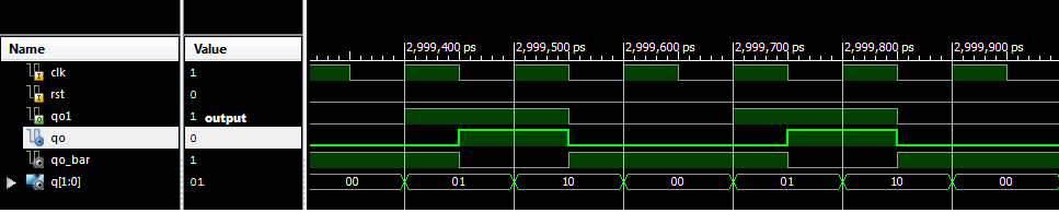
Simulation Results:

RTL schematic:

Do write back to me for more details on FSM coding at verilogblog@gmail.com.. have a nice day


