Most the FPGA boards these days come to high frequency oscillators in orders of 50Mhz/100Mhz and the circuits which we have to drive using FPGA work on lower clock rates. So clock division is the need for such applications. Though Xilinx provides DCM IP cores for clock division, they are board specific and appear as a black box. With the counters explained below you can customize your code and synthesize it as per your requirement which are independent of the board you use.
Divide by 2 counter :

Its one of the simplest and most used counter which requires only one D-Flip Flop. We have to first design a D-FF and connect the Q-bar output to the D input to get division by 2. Waveform based simulation can be used to verify your design. You can notice that the o/p will have 50% duty cycle too.
Given below are the code with RTL schematic created using PlanAhead tool. You can verify the code for and the RTL.
RTL/CODE:

Simulation results:

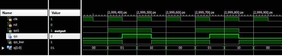
Divide by 3 counter :

1. mod 3 counter
2.Dff
Dff code has to be modified in this case as the FF has to be transparent to D only on the negative edge of the clock..
With slight modification for the D-FF code we can create the DFF for neg- edge. We have to use a OR gate to get the final o/p. The RTL gives the clear design for divide by 3 counter.
RTL/CODE:

simulation results :
Divide by 4 counter :

If you notice , the design for divide by 4 is similar to the divide by 2. Here we have two divide by 2 counters in cascade. This situation makes our efforts easy as we don't have to rewrite the code for div4 counter. All we have to do is to instantiate the div2 counter twice and connect them is cascade as shown. Here there is no need of any other logical gates like in case of Div3 counter. Refer to the code and RTL for div3 counter as shown below. Individual reset are used for the DFF and they must be set in order. First the D-FF X1(rst1) must be reset(high) and then turned low. Next you have to reset the D-FF X2 high followed by low.
RTL/CODE:

simulation results :

Once the deign for divide by 4 is complete you can extend the same concept for all mulitple of 4 division like 4,8, 12 etc. Only modification you require is the number of D-FF stages. For divide by 8 counter you need 3 D-FF in cascade and for 12 you will need 4 and so on... Below are the design for 8 and 12 counters . Try and design it with the same codes and instantiate them accordingly.

Divide by 6 counter :

Not much complex , just 3 D-FF and cascading them gives us divide by 6 counter. Coding is quite simpler as compared to divide by 3 counter. Try and code it yourself if you get stuck , you can refer my code below with RTL schematic.
RTL/CODE:

Simulation results:

We will update the remaining counters as and when the design is ready. Thank you . Keep reading .
RTL/CODE:

Simulation results:
We will update the remaining counters as and when the design is ready. Thank you . Keep reading .
please update divide by 3 counter using 25% duty cycle
ReplyDeletehttp://verilog-code.blogspot.com/2018/08/books-to-buy-for-beginners-verilogvhdl.html
Delete